PCB Business Card
Business card that acts as a spectrum analyzer and BLE sniffer with built-in NFC.
- Published
- Length
- 18 min read
- Views
- …

Contents · 11 sections
How do you stand out in a recruitment cycle? Companies get thousands of applicants, many being very qualified. As an applicant, you spend hours writing short answer responses, re-entering your education and personal background, just for the company to maybe respond in a week, or a month, or months, or even over half a year later. Do this x100 times, and it gets tiring really quickly.
You can talk to recruiters at recruitment events, but end up waiting in a long line of other applicants to get your two minutes of fame with the recruiter. And when you finally get to talk, they take your resume and place it on top of tens of others on their clipboard, each glowing under the dim gym lights with different parts marked up with a highlighter. You made your resume purposefully boring in style, because you know, at the end of the day, they’ll just run this through a scanner and feed it to an ATS reader for some LLM to judge. A few applicants later, and you can only hope the recruiter still knows your name. This is not the fault of the recruiter or company; there are just so many applicants these days.
There’s not a lot of room for creativity. Resumes and CVs have quite a standard format, and are made to be information dense: 10x tokens saved after creating novel LLM harness to manage Agile workflows bla bla bla… This is what I thought, until I saw a YouTube video about a custom PCB business card, and started researching this.
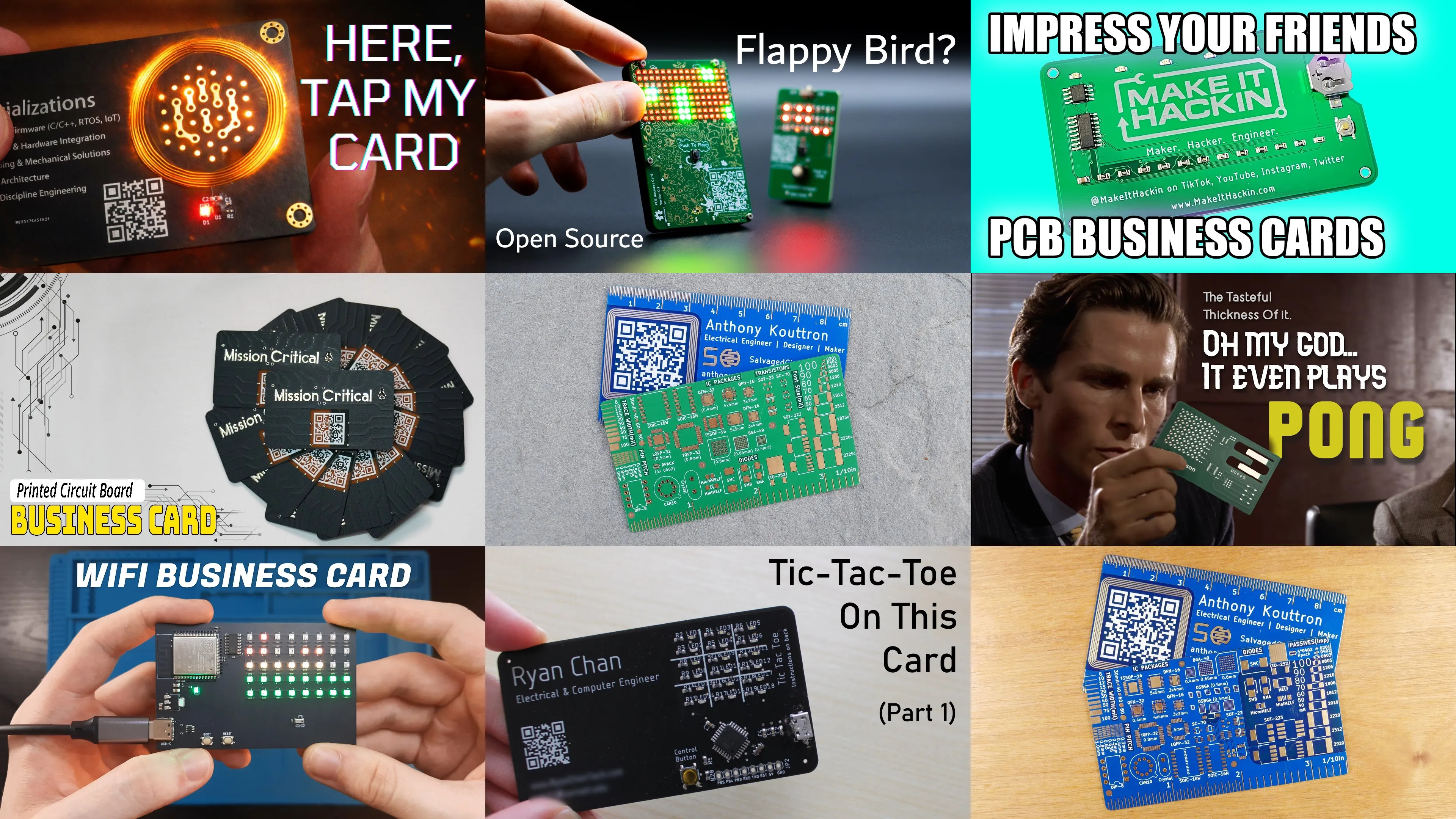
So you’re saying I get to not only show off my engineering skills, but also work the right side of my brain and add in my own creative mix? Sign me up! No PCB business card is the same, each a reflection of the engineer’s interest, so to that end, I spent quite a bit of time pondering on what I wanted to build.
so… what does it do?
It’s a spectrum analyzer. The array of 8 LEDs divides up the 2.4GHz spectrum band, and glows according to how much power is on each band. Start playing some music over Bluetooth, and you’ll see more activity over the Bluetooth portion of the spectrum. You can get a sense of how much noise some WiFi channels have to help pick the right 2.4GHz band. The microcontroller on the board also supports Bluetooth, so plug it into your laptop and start using it to sniff or send BLE packets. With GPIO and ST-Link broken out, you can reflash this board and use it as a battery-operated microcontroller for an IoT project.
There is an NFC coil on the front, so you can tap the card to see who made it (me!). A ruler on the back for quick measurements, alongside common SMD footprints so you can gauge how much space an IC will take. And, of course, a cat to remind you about the species that actually rules the world.
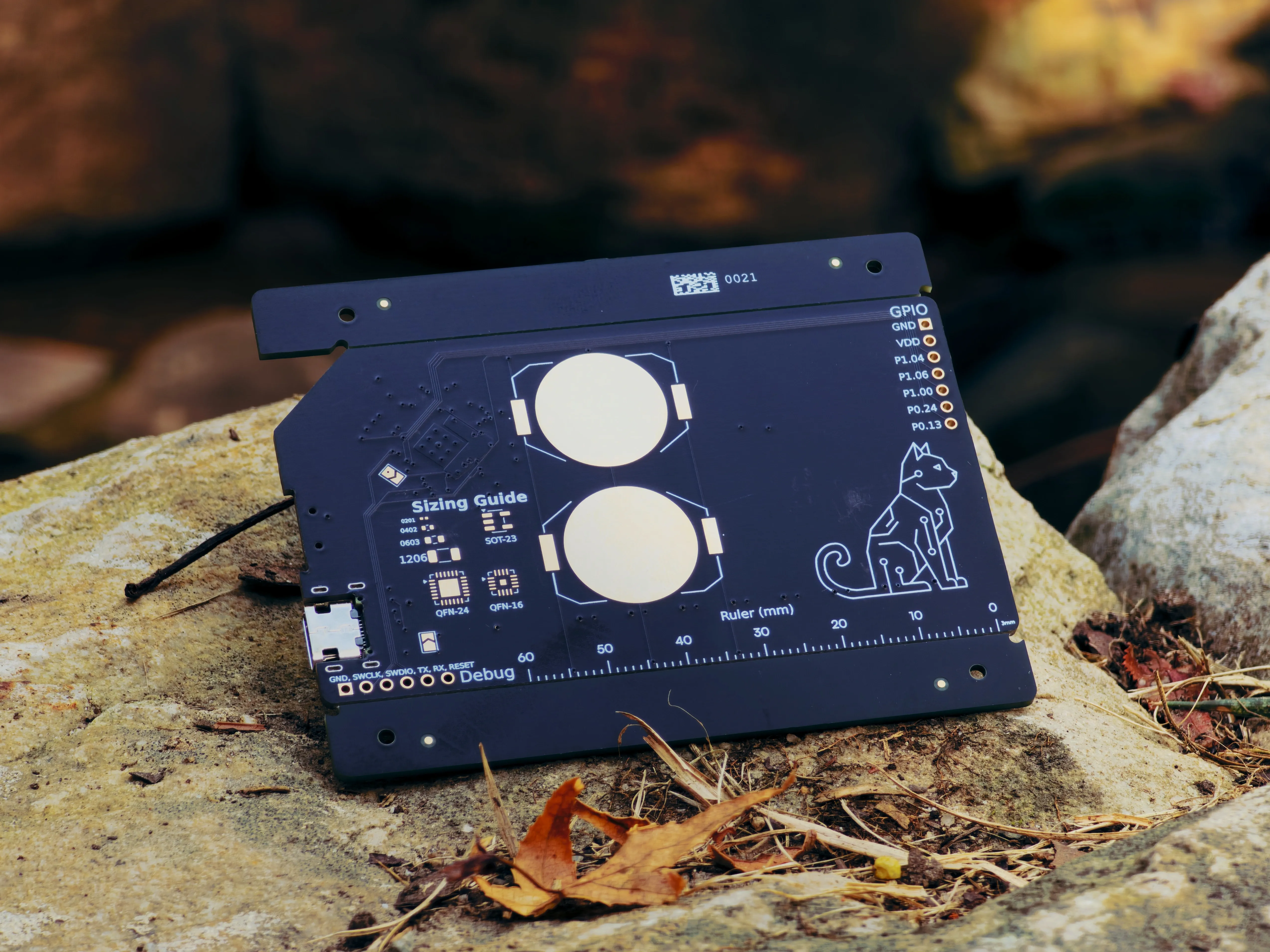
The board contains two small trace antennas and a Nordic nRF52840. One antenna is tuned for NFC at 13.56MHz, with the other antenna tuned for 2.4GHz. The nRF52840 supports a range of 2360MHz to 2500MHz across multiple protocols: Bluetooth Low Energy (BLE), Bluetooth mesh, Thread, Zigbee, IEEE 802.15.4, ANT/ANT+, and Nordic’s proprietary 2.4GHz wireless protocols.
The IEEE 802.15.4 support is what allows this board to run as a crude spectrum analyzer, as the standard requires the radio to perform RSSI detection on a channel to find the one with the least interference. For the card, I used that energy detect function to measure the energy within 5MHz channel buckets.
why
Out of the existing PCB Business Cards, the ones I found coolest are the ones that are interactive. And while games are cool and quite addictive, I very quickly had my mind set on building something that gave you another perspective on the world; something that showed you the environment in ways you can’t normally see.
Recently I’ve been doing a lot of RF-related work, with projects like the 3.4GHz Live Video transmission system I built for Duke Aero. At DEF CON, I saw a talk about someone who tried using a Bluetooth sniffer to attack a storage locker.
So naturally, my mind went towards a spectrum analyzer, enabling card wielders to see the invisible radio signals that allow Bluetooth, WiFi, and other appliances to work. And it’s interactive, in that you can start a download over 2.4GHz WiFi, or start using your Bluetooth earbuds, and the corresponding lights will jump to life.
how (hardware)
I started with deciding what microcontroller to use, and needed something super low power. ESP32s are quite efficient chips with wireless, but still not efficient enough, since the CR2032 coin cell battery only has a capacity of around 230mAh. When you need efficiency, you go Nordic. They make some seriously efficient chips, with the nRF52840 only needing like 5-10mA during radio transmissions compared to the ESP32 family, which needs around 10x that. Same goes for sleep, an ESP32 typically draws 5-10uA compared to nRF52840 with only 0.5uA of deep sleep current draw. The nRF52840 also supports NFC so I can save some components on the BOM.
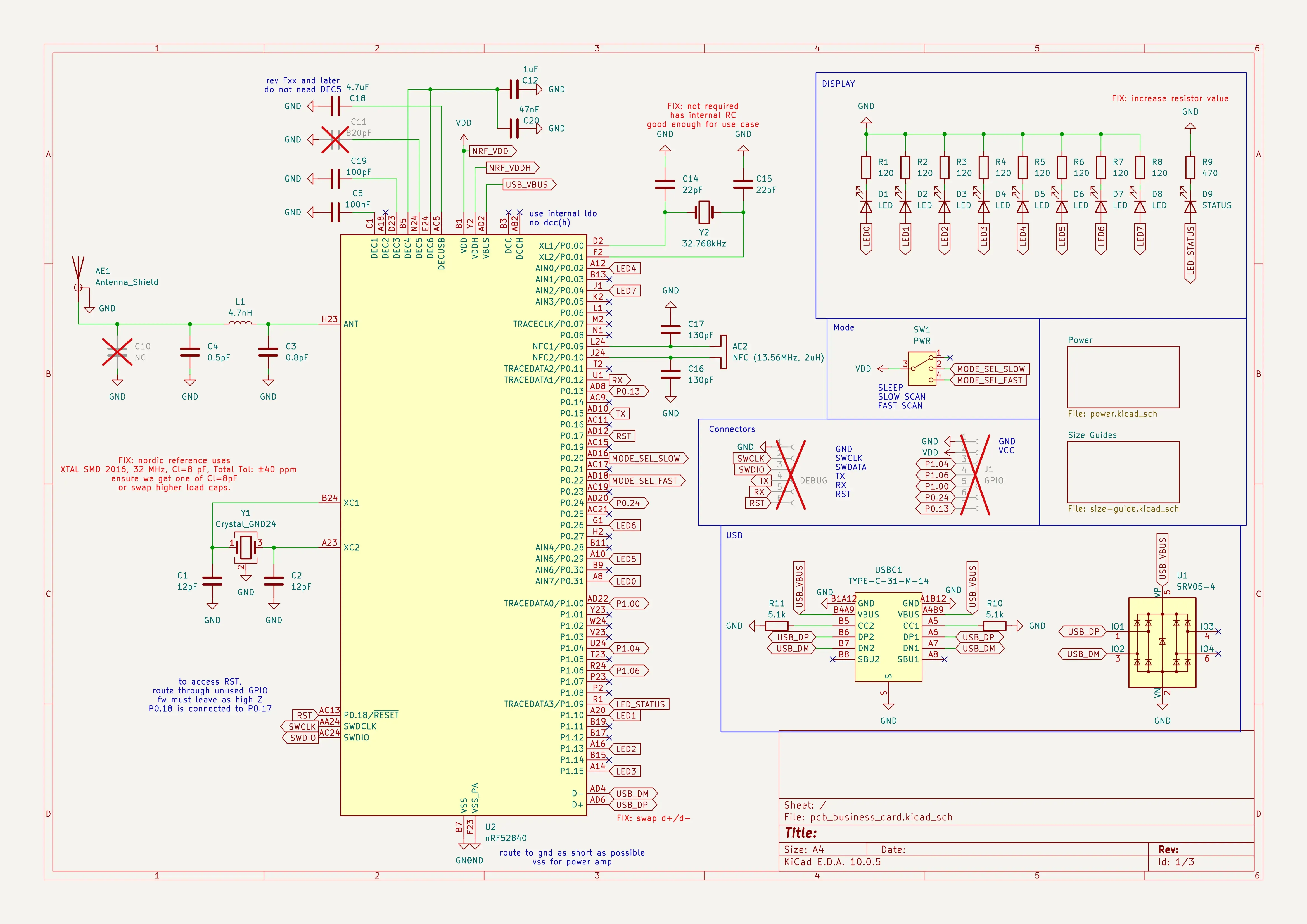
The schematic was quite straightforward. I started with the example schematic provided by Nordic in the datasheet, and created a simple LED array.
powering the board
This was a tough challenge. LEDs draw a lot of current, with the ones spec’d having a forward voltage . This will be powered by a 3.3V battery, but with drops (explained later), let’s say . I would like the LEDs to be bright enough to see within outdoor lighting, so I purposely underspec’d the resistor with . Since the forward voltage of the LED is a range, we’ll use the smaller number as a conservative guess.
A single CR2032 has a continuous discharge rating of , with a maximum rating of around . Hopefully you can see the problem here: we have nowhere near enough current to drive all 8 LEDs, which led me to explore many options.
1. small lithium battery
A lot of small devices have moved away from using coincells, just having a small internal LiPo battery, with these batteries having much higher discharge current.
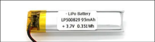
This 5mm battery from PolyBattery.com is rated for 95mA of current, over 10 times more than the coin cell! But, even at 5mm it is still about 1.5x the thickness of the CR2032 battery, and the capacity is nearly a third of a single CR2032 battery. Can we do better?
2. even smaller lithium battery
Turns out batteries can get really, really small.
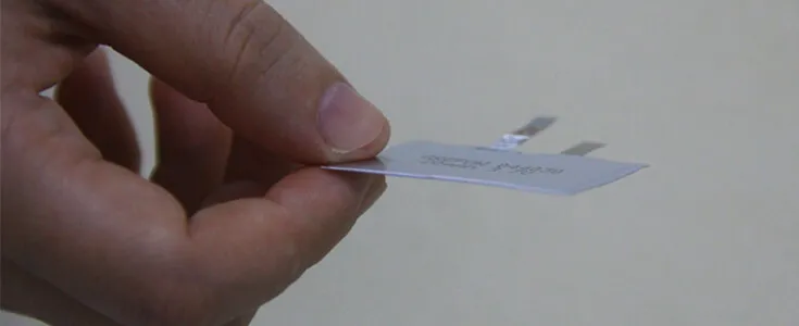
That battery is 0.4mm thin; zero. point. four… While I couldn’t find discharge numbers for these specific batteries, generally they are anywhere from 0.5C to 1C, which equates to around 15mA to 30mA for their 30mAh battery. Again, current is better, but the capacity maxes out at 30mAh for their 0.4mm thin batteries.
| Part Num | Capacity (mAh) | thickness (mm) |
|---|---|---|
| LP044050 | 30 | 0.4 |
| LP103035 | 50 | 1.0 |
| LP094034 | 58 | 0.9 |
| LP202430 | 85 | 2 |
| LP202060 | 100 | 2 |
| LP201256 | 112 | 2 |
| LP204965 | 600 | 2 |
| LP203180 | 800 | 2 |
Abridged table. Numbers sourced from www.lipolbattery.com on Sep 7, 2026 at 10:29 PM EDT, sorted by capacity.
So I’d have to jump up to 2mm thickness to get a workable capacity, which is still quite thin, but using pouch batteries introduces a new hazard: fire. If a lithium battery gets punctured, it can experience thermal runaway, leading to an unscheduled rapid combustion event. I don’t want to be giving people boards that have the same failure mode as the iconic Samsung Galaxy Note 7.
Coin cell batteries have a hard shell around them to help prevent punctures. I could wrap the battery with some 3D-printed case, but this adds a lot of complexity, thickness, and these batteries are not as cheap and widely available as CR2032s anyways, so I scrapped the route of using lithium pouches.
LR/LIR batteries
The naming behind CR2032 is purposeful. That CR represents lithium manganese dioxide chemistry (C) and being round (R), and 2032 denotes 20mm diameter and 3.2mm thickness. There are also LR2032 and LIR2032 batteries that use rechargeable lithium-ion chemistry, with about 0.2C to 0.5C of discharge current, maxing out at 1C. Standard cells are 45mAh so this means ~9-20mA of standard current, with peaks of 45mA.
And these have the benefit of being surrounded by a hard shell, so they’re safer, but they only have a capacity of 45mAh. Furthermore, designing around this as a requirement may lead to cases in the future when a user swaps the battery, not knowing it must be lithium-ion, and end up confused as why the board will not function.
two batteries
The solution I landed on was to just use two CR2032 batteries (wired in parallel) and some smart light scheduling to reduce the current draw. I’ll go over this in more detail in the firmware section. Optionally, an LR2032 battery can be used; the circuitry allows for the higher voltage of those cells.
the power mux
The board has two methods of being powered. One is the aforementioned battery, and the second is via the USB port. My original revision, for simplicity, left power unplugged from USB, relying entirely on battery power, but for the second revision I decided to actually invest in building a power mux.
I cannot just wire the two lines together, since that means sending 5V to a 3V coin cell battery when plugged in, and also potentially sending power back to the USB host. For this job, there exist power mux ICs that I could add to the board, but this method is costly as these parts are not likely to be found as “basic” parts for JLC assembly (meaning I need to pay an additional fee for the part). Thankfully, this problem can be solved pretty easily using a transistor:
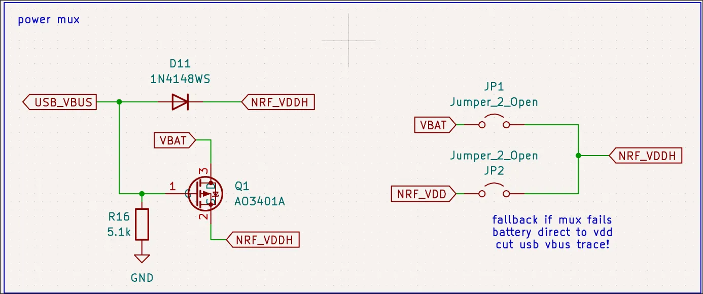
A P-channel MOSFET turns on when its gate voltage is lower than the source.
When USB is disconnected, the gate is pulled down to 0V, which is lower than
VBAT of 3V, so the Nordic chip gets 3V on VDDH. When USB is connected, USB 5V
is tied to VDDH via a diode, and the gate will sit at 5V. This is higher than
VBAT’s 3V, so the MOSFET turns off. I added a few pads that I could short to
bypass this functionality if something didn’t end up working, but ended up not
needing that (thankfully!).
Click me to test this out yourself!
The nRF52840 has a built-in LDO to drop voltage, with a register to control the output voltage. For those unaware, an LDO is akin to a variable resistor with the goal of maintaining a lower output voltage. The chip operates on 1.3V-3.3V, and this LDO allows the board to take up to 5V without needing external circuitry. Other than that, the board is quite simple. A 3-pole switch to choose the mode (off, slow scan, fast scan). A USB port with a TVS diode. Some exposed GPIOs so this card can be repurposed as a general MCU.
board layout
The layout is also quite simple. I started with the RF antenna, using TI’s SWRA117D trace antenna, placing it at the corner of the card. I then oriented the nRF52840 so that its antenna pin has a straight uninterrupted path to the antenna, simplifying the RF engineering required, and used JLC’s impedance calculator to figure out the required trace width for a transmission line. The matching network was the reference one given by Nordic in their documentation, as I do not own a VNA to characterize these boards.
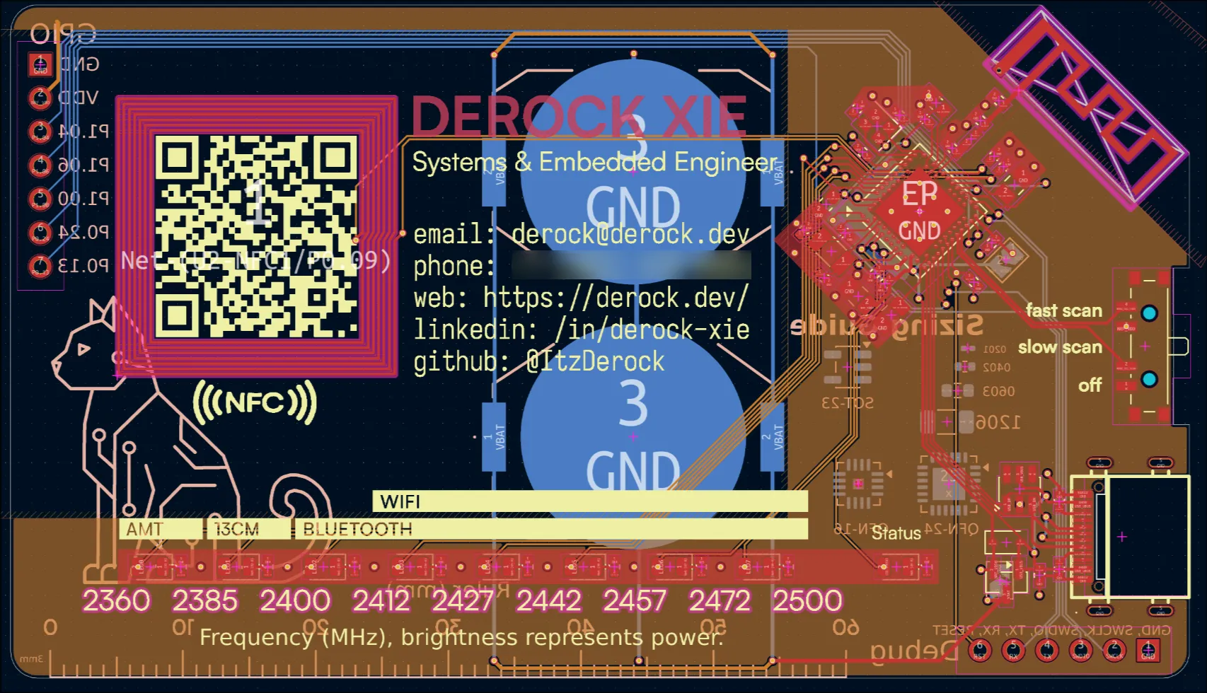
NFC operates at a substantially lower frequency than 2.4GHz, so its layout is less strict. I routed them as if they were differential pairs, so close together, but didn’t care too much about length matching. Unlike the TI 2.4GHz antenna trace, which uses the nearby ground plane as the other half of the dipole structure, the NFC trace expects no copper around it. Having a fill nearby can detune the antenna, so I added a keep-out zone as big as I could reasonably fit. I’m not chasing maximum range, as long as the antenna stays tuned enough to still work at close range, it will be fine.
Everything else is quite textbook; decoupling capacitors near all the VDD pins, 4-layer board with signal, gnd, pwr, signal, and a set JLC stackup for predictable impedance.
silkscreening
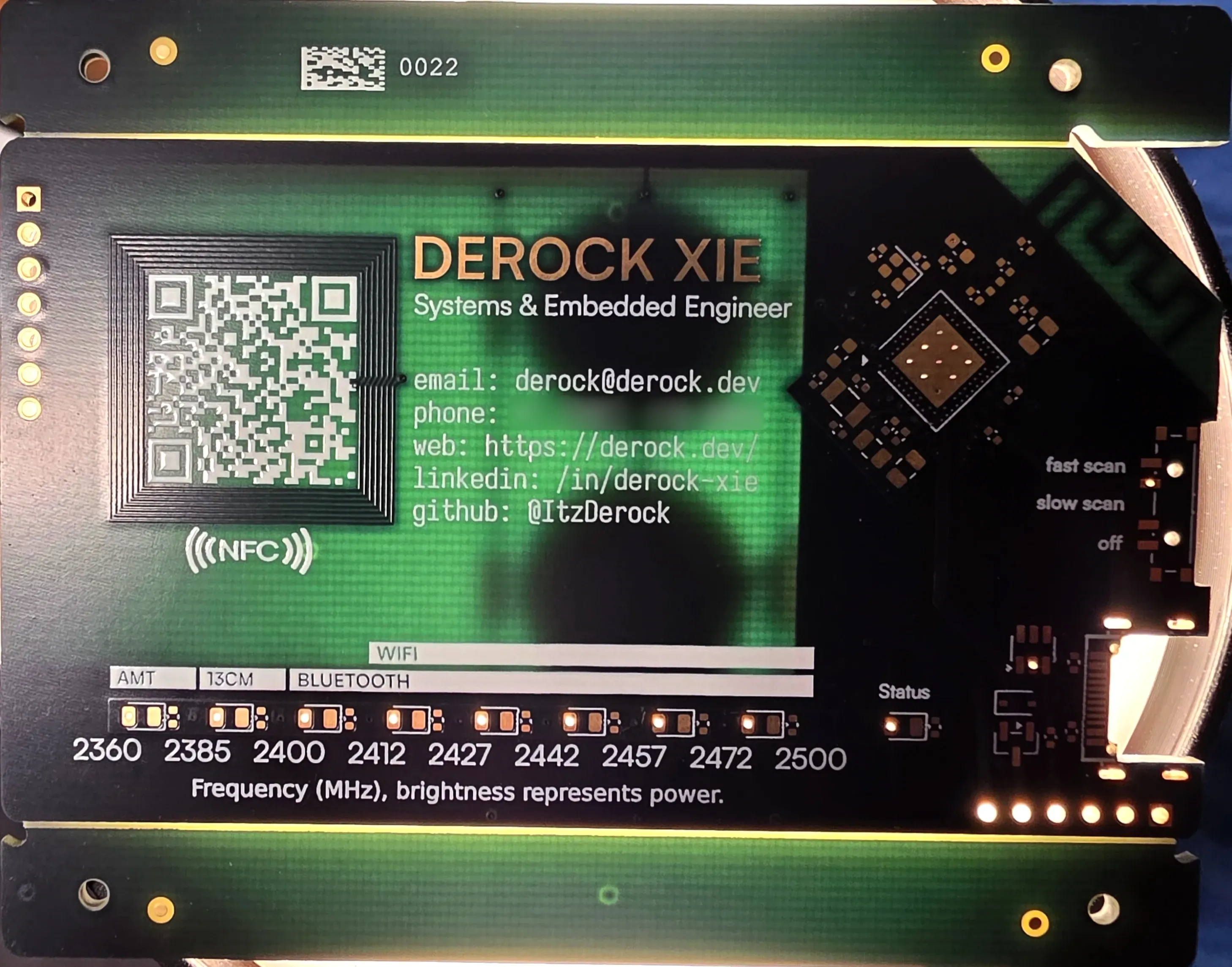
KiCad’s silkscreen drawing tools are quite limited, so I used Inkscape to draw the silkscreen and imported it as an SVG into KiCad. I selected a black substrate on JLC, and white for the silkscreen.
To get a gold finish on my name, I typed my name out and used it to create a fill, not connected to anything. Normal finish is silver, so I opted for an ENIG surface finish for the gold color.
how (firmware)
I’ve been using Rust more, and have started falling in love with the language. The firmware for this card is built using Embassy, a Rust-based and async-friendly framework that supports many MCUs, including the nRF52-family.
The firmware is also quite simple, with everything revolving around a finite state machine. The state is reconciled at boot based on GPIO position, USB status, and NFC status. The board lives normally in deep sleep, with edge-triggered interrupts set for the 3-pole switch on the side, USB, and NFC.
Embassy’s radio support is not as thorough as I’d like though, and is a pretty
heavy abstraction, so for spectrum-analysis tasks, I talk with the radio
directly via the Peripheral Access Crate (PAC). It’s a slight abstraction over
setting bare register values, allowing me to write code without having to wrap
everything in an unsafe block:
/// Single ED sample at current frequencypub async fn sample_ed(&self) -> i16 {    // ramp up if not already ready.    if self.state() != State::RX_IDLE {        self.r.tasks_rxen().write_value(1);        self.wait_ready_state(State::RX_IDLE).await;    }
    self.r.events_edend().write_value(0);    self.r.tasks_edstart().write_value(1);    RADIO_EDEND.wait().await;
    let sample = self.r.edsample().read().edlvl();    self.disable().await;
    // datasheet for nRF52833 says ED_RSSIOFFS + VAL_{HARDWARE}    // but nRF52840 scales by ED_RSSISCALE    // that makes no sense, EDLVL max is 127 => +415 dBm which is absurd    // so just use the offset.    ED_RSSIOFFS + i16::from(sample)}
In the above sample, self.r is the radio peripheral from nrf_pac. Most
example code for the radio has the main CPU poll the radio to see if it is
ready, but we can do better using interrupts.
// Handle radio ISRspub struct RadioISR;impl typelevel::Handler<typelevel::RADIO> for RadioISR {    unsafe fn on_interrupt() {        let radio = embassy_nrf::pac::RADIO;
        // check registers to see what changed        if radio.events_ready().read() != 0 {            radio.events_ready().write_value(0);            let state = radio.state().read().state();            RADIO_READY.signal(state);        }
        if radio.events_edend().read() != 0 {12 collapsed lines            radio.events_edend().write_value(0);            RADIO_EDEND.signal(());        }
        if radio.events_end().read() != 0 {            radio.events_end().write_value(0);            RADIO_END.signal(());        }
        if radio.events_disabled().read() != 0 {            radio.events_disabled().write_value(0);            RADIO_DISABLED.signal(());        }    }}
To sweep the spectrum, I just update the frequency, take a sample, and repeat. Then I collect it all into the 8 buckets defined on the silkscreen.
led scheduling
Previously I mentioned how the board is quite current limited due to the battery limits. If all eight LEDs were active, we would completely saturate the battery, causing its internal resistance to increase enough to where the voltage drop will cause the chip to brown out.
Unless you are in a very, very, very congested area, you will not see 100% utility on all bands. More likely there will be like 2-3 buckets with 20% activity, and the rest idling. If you add that up, it’s equivalent to having one LED run at utilization. This is already great in itself, but we can do even better.
To control brightness, PWM is used. The LED pin is driven high for a very brief period, then driven low for the rest of the period, with the cycle repeating 800 times per second. If we stagger the on period for each LED, from the battery’s perspective, only one LED is ever active at a time. Our slow human eyes do not see this flickering, and just see the LED as normal.
Implemented in firmware, it looks something like this. It’s a basic greedy scheduler, handling the duty cycles in order of highest to lowest.
/// Greedy peak-minimizing scheduler.////// `buckets[i]` = duty required for LED `i`, in units of 1/SCHEDULING_MAX,/// and must already be sorted greatest-to-lowest////// Returns `[(phase_offset, duty); N]`, same index order as input./// `phase_offset` and `duty` are both in units of 1/SCHEDULING_MAX of the period.fn schedule_phases<const N: usize>(buckets: [usize; N]) -> [(usize, usize); N] {    debug_assert!(        buckets.windows(2).all(|w| w[0] >= w[1]),        "buckets must be sorted greatest to lowest"    );
    let mut load = [0u32; SCHEDULING_MAX];    let mut prefix = [0u32; 2 * SCHEDULING_MAX + 1];    let mut out = [(0usize, 0usize); N];
    for (i, &raw_duty) in buckets.iter().enumerate() {        let duty = raw_duty.min(SCHEDULING_MAX);        if duty == 0 {            out[i] = (0, 0);            continue;        }
        // Unroll load[] once around the circle so every circular window        // [offset, offset+duty) becomes a flat range sum via prefix[].        for k in 0..(SCHEDULING_MAX + duty) {            prefix[k + 1] = prefix[k] + load[k % SCHEDULING_MAX];        }
        // Pick the offset whose window has the least total overlap.        let mut best_offset = 0usize;        let mut best_sum = u32::MAX;        for offset in 0..SCHEDULING_MAX {            let sum = prefix[offset + duty] - prefix[offset];            if sum < best_sum {                best_sum = sum;                best_offset = offset;                if sum == 0 {                    break; // zero overlap is optimal, stop early                }            }        }
        // Commit this LED's window into the load map.        for k in 0..duty {            load[(best_offset + k) % SCHEDULING_MAX] += 1;        }
        out[i] = (best_offset, duty);    }
    out}
One consideration must be made though. We (humans) do not perceive brightness in a linear manner, instead following a logarithmic curve. A linear 20% duty compared to 40% does not result in us seeing the second as double the brightness. Following the CIE 1931 curve, this results in a jump from perceived lightness of to , so to get the display to look correct, we must correct for this human limitation.
/// Translates a linear relationship to perceived human brightness/// Follows CIE 1931 curve////// Input: 0..=SCHEDULING_MAX, output follows same range.fn linear_to_perceived(raw_duty: usize) -> usize {    let m = SCHEDULING_MAX as f32;    let x = raw_duty as f32;    let alpha = 0.08 * m;
    let y = if x <= alpha {        x / 9.033    } else {        let norm = ((x / m * 100.0) + 16.0) / 116.0;        norm.powi(3) * m    };
    y.round() as usize}
Since I have the compute, I used the full CIE 1931 curve. You could optimize this with a LUT instead, but the nRF52840 has a floating-point unit and runs at 64MHz, so it performs these calculations without breaking a sweat.
bluetooth
soon™️
It’s currently WIP; there will be (basic) Wireshark support, so you can use this board as a BLE sniffer. I’ve tested sending advertisements, and my phone is able to receive them, validating the RF path.
what’s the damage
Production of these boards was not cheap, and I had to order two revisions because I had flipped D+/D- for USB and used the wrong symbol for the crystal, leading to some funky behavior as one of the crystal pads was disconnected.
I ordered 30 boards, with 10 being assembled.
| Line item | Qty | Total Cost |
|---|---|---|
| PCB Manufacturing (Black FR-4 substrate, ENIG finish, JLC04161H-7628 stackup) | 30 | $77.00 |
| PCB Assembly Setup Fee | 1 | $25.56 |
| PCB Assembly Stencil | 1 | $8.25 |
| PCB Components (nRF52840, capacitors, LEDs, etc. NO battery holder or switch) | 10 | $71.80 |
| JLC Extended Parts Fee | 1 | $35.19 |
| SMT Assembly Fee | 1 | $3.62 |
| PCB Assembly Fixture | 1 | $16.42 |
| Packaging Fee | 1 | $0.49 |
| X-ray Inspection | 10 | $16.40 |
| ➡️ SUBTOTAL | NA | $254.69 |
| Shipping | NA | $4.37 |
| VAT | NA | $24.57 |
| Discount (coupon) | 1 | -$9.00 |
| PayPal fee | 1 | $1.37 |
| ➡️ TOTAL | NA | $276.00 |
A good portion of the charge is just assembly fees and extended parts fees. If I placed a larger order, the rate per board would go down, but I am not made of money so I settled on the 30 boards, 10 assembled balance. Additional savings could be made by removing the LFXO (low-frequency clock) since the nRF52840 supports using an internal (though less-accurate) RC circuit in lieu of an external oscillator. I also opted for some fancier flush USB-C receptacles, instead of regular surface mount ones, so the BOM can be reduced by using a more standard part there. For just the parts, each board is just shy of $10.
Two components needed to be hand-soldered afterwards as they weren’t available through JLC: the battery holder, and the switch. I purchased those from Mouser.
conclusion
Overall, this is a 10/10 project. This is my first time building a board handling RF, so I got a lot of experience handling layout and running all the required calculations. I also got more experience with Embassy and Rust, and can say that I am quite Rust-pilled. And I love that I have a cool board I can show off to people.